



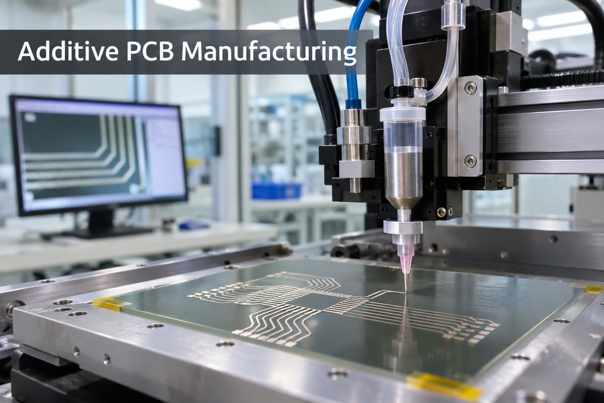
Additive PCB manufacturing builds conductive or dielectric features only where they are needed instead of starting with a continuous copper layer and removing unwanted metal. Depending on the technology, a process may print conductive ink, dispense paste, plate copper selectively or combine printed layers with conventional components. It can shorten iteration cycles and reduce material removal, but it does not automatically equal conventional multilayer PCB performance.
The engineering question is not “additive or subtractive?” in isolation. It is whether the complete material system—substrate, conductor, dielectric, surface preparation, curing and inspection—meets electrical, mechanical, thermal and production requirements.
What Is Additive PCB Manufacturing?
In a subtractive process, copper-clad laminate is imaged and etched. In an additive process, conductive material is deposited or grown in selected locations. Semi-additive processing uses a thin seed layer, patterns resist, plates the required copper and removes the remaining seed. Printed-electronics processes may instead deposit silver, copper or other functional inks by inkjet, aerosol jet, screen printing or dispensing.
| Process family | How conductors are formed | Typical strength | Main limitation |
| Subtractive | Remove unwanted copper from clad laminate | Mature PCB materials and supply chain | Etch undercut and removed material |
| Semi-additive | Plate copper into patterned openings over a seed layer | Fine-feature copper structures | Seed, adhesion, plating and stripping control |
| Printed conductive ink | Deposit ink or paste and cure/sinter it | Digital pattern changes and nontraditional substrates | Conductivity, adhesion, curing and environmental stability |
| Multimaterial 3D printing | Alternate dielectric and conductive deposition | Embedded or non-planar functions | Material compatibility, resolution and qualification |
Detailed Process Parameters and Their Practical Meaning
Published machine capability is not a finished-product guarantee. Fraunhofer ZSI describes a dual-inkjet system using an epoxy dielectric and silver-nanoparticle conductor, with reported technical possibilities down to 75 µm track width and 17 µm track thickness for that specific system. Those figures must not be generalized to every printer, ink or substrate.
| Parameter | What to record | Why it changes the result |
| Feature geometry | Printed width, spacing, thickness and edge variation | Controls resistance, density and risk of opens/bridges |
| Ink or paste | Material, solids, viscosity, particle size and storage condition | Affects jetting, spreading, sintering and conductivity |
| Substrate | Material, surface energy, roughness, temperature limit and CTE | Controls wetting, adhesion, dimensional stability and cure window |
| Deposition | Drop size, pitch, passes, speed, nozzle condition and environment | Changes thickness uniformity and line definition |
| Curing/sintering | Method, temperature, time, atmosphere and ramp | Determines final resistance and substrate damage risk |
| Inspection | Geometry, sheet resistance, adhesion, continuity and environmental tests | Separates a printed pattern from a qualified interconnect |
Additive PCB Manufacturing Step by Step
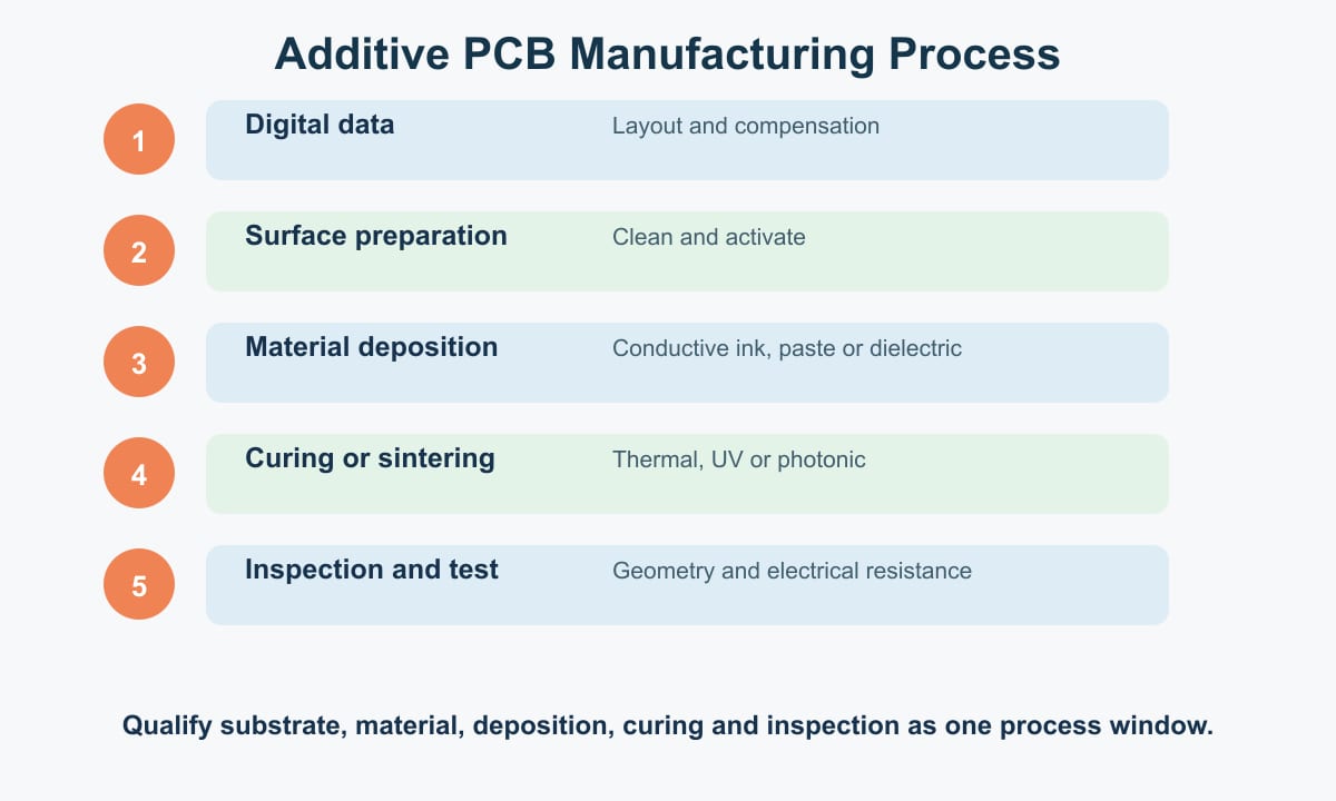
- Prepare digital data. Convert the circuit pattern into compensated deposition paths, registration targets and layer sequences.
- Prepare the surface. Clean, activate or prime the substrate so the selected material wets and adheres consistently.
- Deposit functional material. Control nozzles, screens or dispensing paths, then inspect for missing, merged or unstable features.
- Cure or sinter. Convert the deposited material into a stable conductor or dielectric without exceeding substrate limits.
- Build additional layers if required. Align conductor and dielectric layers and create vertical connections through the qualified process.
- Inspect and test. Measure geometry, resistance, adhesion and continuity; add environmental and mechanical tests appropriate to the application.
Additive vs Subtractive PCB Manufacturing
| Decision | Additive route | Conventional subtractive route |
| Design changes | Digital pattern changes can be fast | Digital imaging is also flexible, but the process remains copper-clad and etched |
| Materials | Functional inks, pastes and printable dielectrics | Established copper foils and PCB laminates |
| Conductor performance | Depends strongly on material and curing | Bulk copper performance is well characterized |
| Geometry | Can support planar, flexible or selected 3D surfaces | Optimized for planar panel production |
| Qualification | Often application- and process-specific | Mature PCB standards and supplier controls |
When Additive Electronics Is a Good Fit
- Rapid prototypes and frequent digital pattern changes.
- Sensors, antennas, heaters or electrodes on flexible or unusual substrates.
- Low-volume customized electronics where tooling dominates cost.
- Functional traces on 3D surfaces when the process supports geometry and registration.
- Hybrid assemblies that combine printed functions with mounted components.
It is a weak fit when the design requires conventional multilayer-board performance, low conductor resistance, mature plated-through-hole structures or a qualification history that the selected additive material system cannot provide.
Common Failure Modes and Root Causes
| Failure | Likely causes | Verification |
| High or unstable resistance | Insufficient thickness, incomplete sintering, porosity or cracking | Four-point measurement and section analysis |
| Poor adhesion | Contamination, surface energy mismatch or incompatible cure | Adhesion testing before and after environmental exposure |
| Bridging or line spreading | Excess volume, low viscosity, poor wetting control | Optical measurement across the panel |
| Open traces | Nozzle dropout, discontinuous deposition or substrate defects | In-process imaging and electrical continuity |
| Layer misregistration | Substrate movement, weak fiducials or alignment error | Registration coupons and dimensional mapping |
Design and Procurement Checklist
- State whether “additive” means semi-additive copper, printed ink or multimaterial 3D printing.
- Define conductor resistance, current, temperature rise and environmental limits.
- Lock the substrate and functional-material system before layout release.
- Specify cured dimensions, not only digital artwork dimensions.
- Agree on adhesion, continuity, resistance and aging tests.
- Build test coupons that represent minimum features and layer transitions.
- Do not assume a printed prototype automatically scales to volume production.
FAQ
Is additive PCB manufacturing the same as 3D printing a PCB?
No. Additive is a broad category. It includes selective plating and printed conductive materials as well as some multimaterial 3D processes.
Can printed conductive ink replace copper?
Sometimes, but not universally. Compare conductivity, thickness, adhesion, temperature, current, flexing, corrosion and long-term stability for the actual material system.
Does additive manufacturing eliminate etching?
Fully printed routes may avoid copper etching. Semi-additive processes can still include seed-layer removal and other wet processes.
What should be tested first?
Start with geometry, resistance, adhesion and continuity, then add thermal cycling, humidity, flexing or other tests based on the use environment.
Sources
- Fraunhofer ZSI — Circuit board printer
- Fraunhofer ENAS — Printed electronics
- Fraunhofer IKTS — Functional inks
For related imaging context, see PCBTRY’s laser direct imaging process guide and 3D printed circuit board guide. For a project review, contact sales@pcbtry.com.
0 Comments